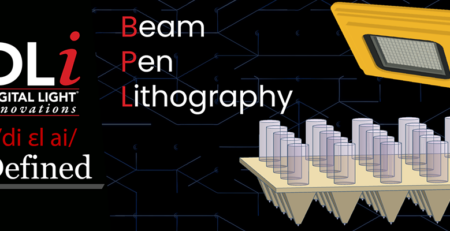
DLi Defined: Polymer Pen Lithography
Amit2023-10-25T19:56:18+00:00As we work our way towards breaking down the structured light-based beam pen lithography (BPL) technique, we have to first look at the direct-write innovation that came just before it. Invented by the Mirkin group in 2008, polymer pen lithography (PPL) took the dip-pen nanolithography (DPN) technique to the next level in nanofabrication.
Nanolithography is a science-based application of lithography, and it is a nanofabrication technique that is used for writing, etching, printing, or modifying materials at a microscopic and nanoscale level. Though not commonly a commercially available technology, nanolithography is commonly used to manufacture semiconductor chips for computers. More recently, nanotechnology is becoming more popular within life science-based applications — including the fabrication of miniaturized chemical and biological systems. With the Mirkin Research Group leading the way in nanomaterial studies, nanolithography techniques and tools are becoming more accessible whilst continuing to expand study of materials science.
The first innovative nanolithography technique was DPN. DPN is centered around the use of high-density cantilever arrays to construct molecule-based patterns. However, these cantilever arrays are also the downside of nanofabrication through DPN. The arrays are not only fragile and costly, but this particular direct-write nanofabrication technique makes it difficult to work within both the micrometer and nanometer scales on a single experiment.
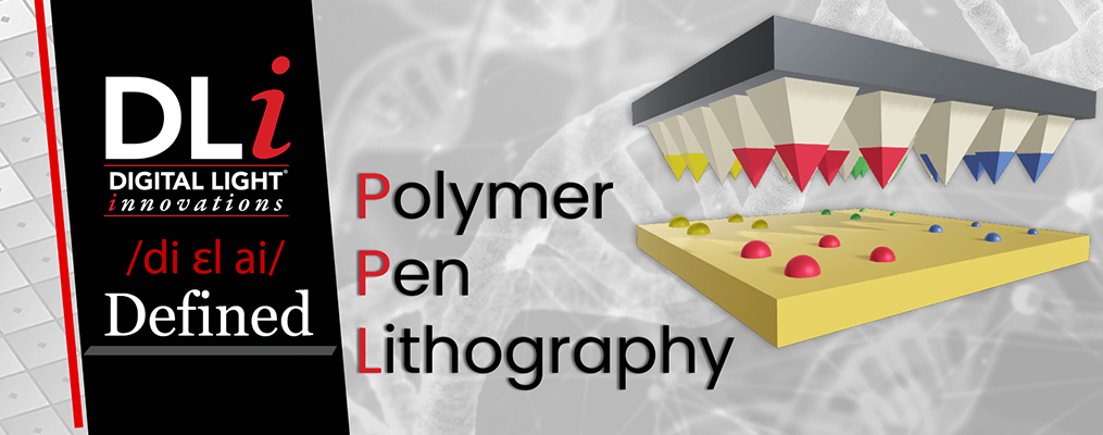
PPL is a cantilever-free scanning probe lithography technique. This means that PPL takes the advantages of DPN while removing the many limitations of a meniscus-mediated ink approach. Instead of tips mounted on individual cantilevers, PPL uses a soft elastomeric tip array.
The PPL tip arrays can contain anywhere from thousands to millions of these pyramid-shaped tips. Their soft nature allows for deformation through increasing the applied force and adjusting the degree of tip deformation. The user has more control over the tip-substrate contact area, which results in a more precise feature size and the ability to generate either nanometer- or micrometer-sized features within one cycle.
The typical PPL array is made from an elastomer that is cured in a silicone mold and then attached to a transparent substrate: such as glass or quartz. After coating the array with ink, the polymer tips will form a dot pattern of the intended structure by directly depositing the ink onto the print surface. Users can change the feature size by varying either the dwell time or the pressure on the tips. Unlike DPN, these pen arrays do not need to be re-inked because the backing of the array acts as a reservoir for the ink.
The world’s first commercialized PPL device was developed by TERA-print. The TERA-Fab M series allows researchers to pattern features across the nanometer, micrometer, and macroscopic length scales within a single tool. The cantilever-free PPL tool fabricates patterns in a high-throughput manner, and allows for pattern designs to be changed on the fly.
As mentioned previously, PPL is not a structured light-based nanofabrication technique, and it does not fully address all of the challenges that come with nanolithography. While improving overall resolution and accuracy from the DPN technique, PPL doesn’t quite offer the precise control or photochemistry-based capabilities that are available through BPL. The advantage of the soft tips reacting to the pressure can also be a disadvantage because the deformations are not always accurate.
That being said, the PPL technique played an integral role in the creation of the award-winning TERA-Fab™ E series product, which utilizes a custom DLi CEL5500 light engine. The .55″ XGA DMD used with the TERA-Fab™ E series allows for individual control of each probe, and that means a more precise print at a higher resolution. With the addition of digital light processing (DLP) technology, the Mirkin Group created yet another approach to improve the nanofabrication process.
By removing the cantilevers, PPL is a cost-effective, direct-write technique that is ideal for life sciences-based applications. With inks ranging from small molecules to synthetic polymers to biomolecules, this lithography technique is perfect for fabricating arrays of soft matter structures such as proteins.
At DLi, we are not only experts in DLP interface and electronic controller board design, but we also specialize in custom optics and prototype development. As we continue to help our partners push the boundaries of light exploration, it is important to look at how DLP can accelerate innovation in new product development. With a custom DLP projector, our partners can create more affordable and versatile technologies — transforming their industry through the use of DLP. Reach out to the DLi team today for your DLP needs.