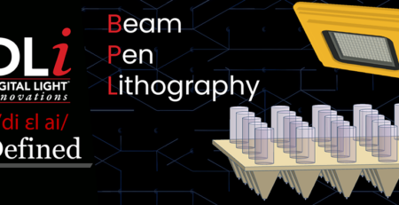
DLi Defined: Dip-Pen Nanolithography
Amit2023-10-25T19:59:25+00:00While Dip-Pen Nanolithography (DPN) is not a structured light application, it is important to take a look at the foundation of nanolithography and how this technology pioneered the path towards Beam Pen Lithography (BPL).
DPN is a direct-write nanofabrication technique. To break it down further, this scanning probe microscopy-based technique uses an atomic force microscope (AFM) tip to create nanoscale patterns by depositing molecules and nanoscale materials onto a solid substrate. AFM tips are used in a similar fashion to fountain pens. The tips are coated with a molecule- or materials-based “ink,” and a water meniscus forms between the scanning probe tip and the substrate surface to transfer the “ink” to the “paper.”
Invented by the Mirkin group in 1999, DPN has been used to write or template a variety of molecules and materials on a variety of surfaces. Some examples include proteins, peptide, DNA patterning, hydrogels, lipids, and many types of biomolecules. The Mirkin Research Group also developed a parallel DPN approach in which they use 2D cantilever arrays to enable large-area patterning. This concept has allowed for DPN technology to contain up to 55,000 pens/cm2.
As a direct-write technique, DPN technology can be set up in either a top-down or bottom-up configuration. A top-down configuration allows the tips to deliver an etch resist to the surface, while the bottom-up configuration delivers the material directly to the print surface via the tips. Either configuration supports a variety of chemistry, materials science, and life sciences applications.
While DPN was the initial breakthrough nanolithography technique, it is currently not the most accessible approach for all researchers. DPN machines are typically mechanically fragile and expensive in comparison to other nanolithography technologies. Additionally, this printing technique requires a highly controlled environment to successfully pattern in (specifically controlling the humidity to manage the size of the water meniscus), and it is a serial process, which implies low throughput. Knowing the drawbacks of DPN, however, has led the way to the creation of additional nanolithography techniques such as Polymer Pen Lithography (PPL) and BPL.
With the addition of structured light, companies like TERA-print have been able to take nanofabrication to the next level. For example, the award-winning TERA-Fab™ E series product utilizes a custom DLi CEL5500 light engine to resolve the scalability and speed issues that are associated with DPN nanofabrication technologies. The .55″ XGA DMD used with the TERA-Fab™ E series allows for individual control of each probe, and that means a more precise print at a higher resolution.
DPN may be perceived as the foundation for an array of scanning probe methodologies, but it is still an active nanofabrication technique that is used to explore new capabilities in biomedicine, chemical synthesis, catalysis, optics, and molecular electronics. What started as a process initially intended for rapid prototyping, transformed into a tool that allowed for advanced materials discovery. This nanolithography technique recently celebrated its 20th anniversary, and it continues to evolve and play an important role in the field of nanotechnology.
At DLi, we are not only experts in DLP interface and electronic controller board design, but we also specialize in custom optics and prototype development. As we continue to help our partners push the boundaries of light exploration, it is important to look at how DLP can accelerate innovation in new product development. With a custom DLP projector, our partners can create more affordable and versatile technologies — transforming their industry through the use of DLP. Reach out to the DLi team today for your DLP needs.