DLi Defined: Beam Pen Lithography
Amit2023-10-25T19:36:26+00:00Knowing the strengths and weaknesses of the direct-write lithography techniques, dip-pen nanolithography (DPN) and polymer pen lithography (PPL), the Mirkin group proposed a more cost-effective and advanced control nanofabrication technique using light.
Nanofabrication is a technique that is used for writing, etching, printing, or modifying materials at a microscopic and nanoscale level. Currently, nanofabrication technology is not widely available commercially, but it is commonly used to manufacture semiconductor chips for computers. Nanofabrication is increasingly being seen more in life science research and optoelectronics as well.
In 1999, DPN was the breakthrough nanolithography technique. DPN uses high-density cantilever arrays to construct molecule-based patterns. DPN is an active nanofabrication technique that opened the door for advanced materials discovery. PPL is a cantilever-free nanofabrication technique that uses a soft elastomeric tip array to directly deposit nanoscale materials onto a solid substrate. Invented in 2008, PPL enables a little more accuracy than DPN because users can better control the applied pressure and force on the tips. Though both of these direct-write techniques have their own advantages in nanofabrication research, these approaches are costly and fragile.
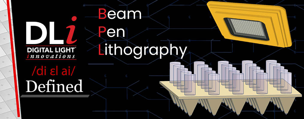
In 2010, the Mirkin Research Group presented a new nanofabrication technique that uses light to affect photochemistry and create nanoscale features. Beam Pen Lithography (BPL) is a cantilever-free lithography approach that is based on PPL. BPL uses a similar array of microscale pyramid shaped tips, but these tips are coated with a thin layer of metallic gold. Small holes are then created at the apex of the tips so that light can be channeled through the ends – exposing the light sensitive material for printing.
The world’s first commercialized BPL device was developed by TERA-print. The award-winning TERA-Fab™ E series product utilizes a custom DLi CEL5500 light engine to take advantage of the capabilities of the DMD. Combined with DLP technology, this product further pushes the boundaries of rapid prototyping with its ability to control light at a sub-wavelength resolution (as low as 250nm) while keeping a 90-95% density distribution across the whole patterning area. With over 30,000 independently addressable pens, the TERA-Fab™ E series was designed to be easy to use for rapid prototyping.
Every innovation we have covered in our DLi Defined series has played an integral role in making nanofabrication more accessible, but BPL was a big leap towards the development of a nanofabrication-based desktop printer. Having affordable technology options for applications such as prototyping circuits, optoelectronics, and medical diagnostics means that researchers in either industrial or academic settings would have the ability to generate structures that span the macro-, micro-, and nanoscales — all in one experiment.
At DLi, we are not only experts in DLP interface and electronic controller board design, but we also specialize in custom optics and prototype development. As we continue to help our partners push the boundaries of light exploration, it is important to look at how DLP can accelerate innovation in new product development. With a custom DLP projector, our partners can create more affordable and versatile technologies — transforming their industry through the use of DLP. Reach out to the DLi team today for your DLP needs.