Fabricating a World with DLP
Joel Coffman2023-10-26T12:04:44+00:00Beam Pen Lithography (BPL) is a recently invented lithography technique that is commonly used to fabricate nanoscale components in applications such as electronics, biology, medicine, and chemical synthesis. Determined to remove the limitations within the current BPL technology, our partners at TERA-print discovered that DLi’s DLP technology would open up new possibilities in applications such as materials design and bioengineering.
DLI’S DLP POWERS THE IMPOSSIBLE – TERA-PRINT’S BEAM PEN LITHOGRAPHY (BPL)
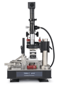
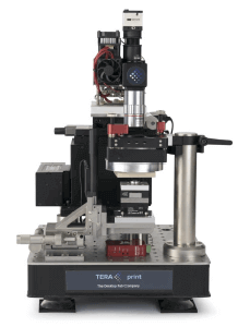
A single digital micromirror device (DMD) can contain over 8 million micromirrors, and each mirror can be switched on or off thousands of times per second. Of course, speed is just one advantage of using Digital Light Processing (DLP®) — many applications can benefit from DLP’s power and brightness efficiency, resolution, and reliable spatial light modulation. As TI’s first DLP design house, the team at Digital Light Innovations (DLi) has extensive experience in creating unique DLP-based solutions for a broad range of applications. One such solution that utilizes a custom DLi-built solution is the TERA-Fab™ E series instrument — the first commercial Beam Pen Lithography (BPL) tool.
BPL is a recently invented photo-lithography technique that is commonly used to fabricate nanoscale components in applications such as electronics, biology, medicine, and chemical synthesis.
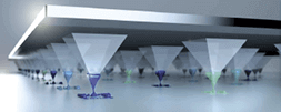
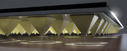
BPL is a cantilever-free scanning probe lithography technique that stems from Polymer Pen Lithography (PPL). Cantilever-based scanning probe lithography techniques, such as Dip-Pen Nanolithography (DPN), have shown great promise for patterning a wide range of materials onto a surface with nanoscale resolution. However, the serial mode of writing and inability to scale the cantilever architecture in a feasible manner, has limited the widespread adoption of these techniques. Rather than using multiple cantilevers with a single pen tip via DPN, PPL uses a two-dimensional elastomeric tip array mounted on a transparent substrate. By effectively eliminating the cantilever and allowing for as many as 11,000,000 pens per array, PPL greatly improves the overall speed and patterning capabilities for scanning probe lithography tools.
BPL is a recently invented photo-lithography technique that is commonly used to fabricate nanoscale components in applications such as electronics, biology, medicine, and chemical synthesis. For BPL, the elastomeric tip array employed in PPL is coated with a thin layer of metallic gold and then nanoscopic apertures are physically or chemically generated at the apex of the tips. Rather than directly printing inks onto a surface with the pen tips like in PPL, BPL directs light through those apertures to expose the underlying photosensitive materials. Importantly, the resolution of this technique is tied to the size of the apertures – the smaller the apertures the finer the structures they can create – and for small enough apertures, this technique ultimately creates nanoscale features with dimensions below the diffraction limit of the light source. Although the use of light in tandem with a BPL array allows for users to perform a multitude of highly localized photoreactions in parallel, this strategy is unable to yield arbitrary patterns over large areas necessary for many photochemical applications because each tip in the array writes the same pattern.
By combining BPL and DLi’s DLP technology into one tool, users can now control light at a sub-wavelength resolution as low as 250nm while keeping a 90-95% density distribution across the whole patterning area. Alongside superior uniformity, the maskless design of the TERA-Fab™ E series platform allows users to easily change patterns on the fly while maintaining high resolution throughout — made possible by the vivid image quality of the DMD.
Determined to remove this limitation and open up new possibilities in applications from microfluidics and bioengineering to nanoelectronics and soft robotics, our partners at TERA-print realized that with the addition of a DMD, a BPL tool would be able to independently control the actuation of each probe. This, in turn, allows users to rapidly generate complex patterns over millimeter-to-centimeter scale areas with nanoscale level precision. They provided the DLi team with their specifications for a DLP system that would bring an unparalleled set of capabilities to their first groundbreaking nanofabrication product, the TERA-Fab™ M series. The M series was released in 2017 as the first commercial maskless PPL tool and, while not a DLP-based system, already allowed for the discovery of new nanomaterials with the ability to pattern a broad range of soft and hard materials in a fast and efficient manner. After receiving a custom-built “CELscope” – a light engine modification combining our CEL5500 light engine and 5x M Plan APO microscope objective – their team expanded their instrument offerings and developed an award-winning TERA-Fab™ E series product that further pushes the boundaries of DLP-based rapid prototyping.
By combining BPL and DLi’s DLP technology into one tool, users can now control light at a sub-wavelength resolution as low as 250nm while keeping a 90-95% density distribution across the whole patterning area. Alongside superior uniformity, the maskless design of the TERA-Fab™ E series platform allows users to easily change patterns on the fly while maintaining high resolution throughout — made possible by the vivid image quality of the DMD.
DLP technology is meant to simplify the complexities of advanced light control and that is yet another strength behind the E series. Harnessing all of its capabilities would normally seem complex or even overwhelming, but TERA-print intended for this system to be straightforward and enable users to start patterning after just a few hours of training. For the first time ever, the discovery, prototyping, and production of nanodevices can be done on a single desktop.
At DLi, we are not only experts in DLP interface and electronic controller board design, but we also specialize in custom optics and prototype development. As we continue to help our partners push the boundaries of light exploration, it is important to look at how DLP can accelerate innovation in new product development. With a custom DLP projector, the TERA-Fab™ E series is a new lithography instrument that is revolutionizing the nanophotonic industry. This versatile rapid prototyping tool is not only easy to use, but is also made affordable through the DLP design. We love seeing our partners succeed in transforming their industry through the use of DLP, and we are excited to see what comes next. Reach out to the DLi team today for your DLP needs.